

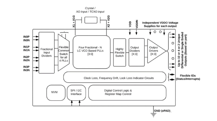
• 12 programmable clock outputs can be generated from a crystal input or any of 4 input reference clocks
• Programmable outputs compatible with LVDS, LVPECL, LVCMOS, CML, and HCSL with programmable signal amplitude
• Independent output supply pins: 3.3 V, 2.5 V, or 1.8 V
• Digitally Controlled Oscillator (DCO) Mode: Frequency step resolution 0.001 ppt, for frequency margining applications
• Internal ZDB Mode with <0.5 ns Input-to-Output delay variation
• OTN/PTN
• BBU/RRU
• 100/200/400G/800G Switch/Router with SyncE support
• Small Cell
• Acceleration card
• Lower phase noise minimizes bit error rate and increases design margin in 56G/112G PAM4 I/O systems
• Better signal integrity increases design margin and leads to faster time to market
• Higher clock tree integration reduces system BOM and increases overall reliability